New institute to redefine AI and semiconductor research at Purdue and beyond
The Institute of CHIPS and AI, launched Nov. 19 in Mountain View, California, in the heart of Silicon Valley, is a pioneering initiative from Purdue University's College of Engineering and the next giant leap in redefining the future of semiconductor and AI research.
The institute's mission is to harness innovative chip technology to power the future of AI while leveraging AI itself to accelerate and improve chip design processes. This approach will not only drive cutting-edge advancements but also address the complexities and costs associated with developing state-of-the-art semiconductor chips. The institute will build on Purdue's long history of leadership and groundbreaking research in projects such as the SRC/DARPA Center for Brain-Inspired Computing and the recently awarded Microelectronics Commons project on AI hardware.

Kaushik Roy, the Edward G. Tiedemann Jr. Distinguished Professor of Electrical and Computer Engineering, speaks during the Institute of Chips and AI launch event in Mountain View, California.
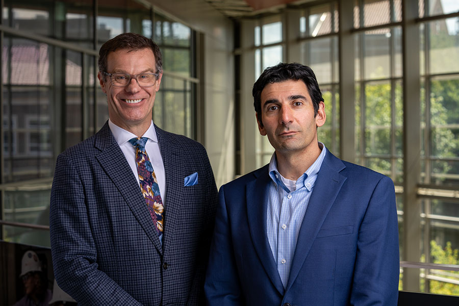
Spearheaded by faculty from the Elmore Family School of Electrical and Computer Engineering (ECE), this newly established institute is directed by Kaushik Roy, the Edward G. Tiedemann Jr. Distinguished Professor of ECE, and co-directed by Anand Raghunathan, the Silicon Valley Professor of ECE. The kickoff event, with strong participation from leaders in industry, government and academia, was a cornerstone of Purdue Engineering's 150th anniversary celebration, which focuses on semiconductors, AI and autonomy.
"The AI revolution began in 2012, fueled by advances in hardware, algorithms and data," Roy said. "Today, as model sizes grow exponentially, energy demands are reaching critical limits. The synergy of AI-driven chip design and chips optimized for AI promises transformative leaps in cognitive computing."
Purdue's rich history of excellence in both AI and chip research led to the university creating the nation's first comprehensive semiconductor degrees program two years ago to address the critical need to train thousands of new semiconductor engineers this decade. The result has been investments from the Department of Defense to lead SCALE, its largest program for microelectronics workforce development, and the decision by the No. 1 global producer of high-bandwidth memory chips, SK hynix, to invest $4 billion to build a new R&D and fabrication facility in Purdue Research Park for advanced memory chips needed to power the next generation of AI processors. This marks the largest semiconductor production facility located at any U.S. university.
"The Institute of Chips and AI joins a host of other Purdue institutes and centers focused on building world-leading programs in physical AI and semiconductor development that reflect Purdue's role as America's semiconductor university," said Arvind Raman, the John A. Edwardson Dean of the College of Engineering. "These programs are inspiring Purdue's efforts to make Indiana the Silicon Heartland."